Product
NEMST-RIE2018 series
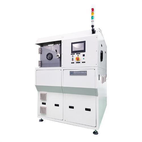
Reactive Ion Etching Plasma Machine
Reactive Ion Etching Plasma MachineFeaturing Design
- Patented High-Density ICP Plasma Source: ~ion density about 1011~1013/cm3.
- Single-side treatment in 1 cycle.
- Unique Distribution Panel Design is employed to ensure uniform plasma generation.
- The bias (DC Pulse or RF) is applied to the product holder.
- An adjustable electrode gap is available.
- Big Area RIE is available.
- End Point Detection is available.
- The system can be configured to a pure ICP source for remote plasma application.
Reactive Ion Etching Plasma MachinePerformances
- Achieves anisotropic etching with high aspect ratios.
- Scalable for 6", 8", and 12" wafers, with a maximum panel size of 660 mm x 660 mm, customizable to client needs.
- Utilizes radicals or ions for high-speed etching.
- Exceptional etching uniformity (reaching 93% or higher).
- Generates high-density plasma under low-pressure conditions.
- Independent control of plasma density and ion energy bias.
Reactive Ion Etching Plasma MachineApplications/Solutions
- Polymer Materials: Polyimide (PI), Parylene, FR4, BT, Teflon (PTFE), etc.
- Silicon-based Materials: Single-crystal Silicon (Si), Polysilicon (Poly-Si), Amorphous Silicon (a-Si).
- Passivation & Protective Layers: Silicon Nitride (Si3N4), Silicon Oxynitride (SiON).
- Dielectric Materials: Silicon Dioxide (SiO2), High-k and Low-k materials.
- Compound Semiconductors: GaN, SiC, GaAs, InP, and other third-generation semiconductor materials.
- Metals & Alloys: Aluminum (Al), Titanium (Ti), related alloys, and barrier metals.
- Special Materials: Sapphire, Diamond, ITO conductive films, PZT piezoelectric materials.
- Advanced Packaging: CoWoS, 2.5D/3D IC, FOWLP, FOPLP.
- IC Substrate Technologies: mSAP (Modified Semi-Additive Process), ABF/BT substrate processes.
- Display Applications: Micro-LED structural etching, surface activation, and cleaning.
- Peripheral Processes: Wafer Reclaim, various types of photoresist removal (Ashing).
- Surface Treatment: Surface activation, roughness improvement, hydrophilic/hydrophobic modification.